
About Us
Cognicatus comes from the Latin cognoscere — to know, to learn, to understand. It reflects our belief that true innovation begins with knowledge. We are not only creating technology, but cultivating intelligence that reaches beyond raw computation to shape smarter, more sustainable systems.
Cognicatus was founded in 2008 by three leading Swedish chip designers – Dr Rolf Sundblad, Dr Staffan Holmbring och Dr Jacob Wikner.
Knowledge at the Core
Cognicatus stands for knowledge-driven innovation. Our work in AI, accelerators, and smart infrastructure is not only about speed or power—it’s about embedding understanding into the systems that shape the future.
Beyond Cognition
The name resonates with our guiding statement: “Beyond Cognition.” While cognition is the act of thinking, Cognicatus expresses a more advanced state: shaping and transforming intelligence itself.

The Meaning of Cognicatus
Chip History
2008
TSMC
80 nm
TSMC 80 nm die, early advanced-node tape-out.
2010-2014
AnaCatum Design
Subsidiary developing mixed-signal ADC architectures (A2DFraming) and Cognitive Converter IP.
2011-2018
SMIC
180 nm (multiple TOs)
Multiple 180 nm tape-outs at SMIC, production and process illustration.
2016
TSMC
180 nm (2 TOs)
Two 180 nm tape-outs at TSMC.
2016
TSMC
55 nm (flash)
TSMC 55 nm flash memory tape-out.
2017
SMIC
40 nm (flash)
TSMC 40 nm flash tape-out.
2018
IMSYS
Accelerators
Joint development program with IMSYS AB on energy-efficient GPU and accelerator technologies for AI workloads.
2019
TSMC
55 nm (mixed)
TSMC 55 nm mixed-signal tape-out.
2019 & 2024
GlobalFoundries (GF) — 22 nm FDX
GlobalFoundries 22 nm FDX tape-outs - FDX / FD-SOI style technology.
2020
TSMC
12 nm
TSMC 12 nm tape-out - significantly denser geometry versus older nodes.
2022
Achronix
GPU–FPGA
R&D partnership with Achronix Semiconductor on GPU–FPGA hybrid architectures for energy-efficient edge compute.
2023
IMSYS
Accelerator prototypes
Energy-efficient GPU and AI accelerator prototypes unveiled with IMSYS AB, developed since 2018.
2025
TSMC
6 nm
TSMC 6 nm tape-out - modern AI/compute oriented processes.
2026
Bris
6 nm · inference
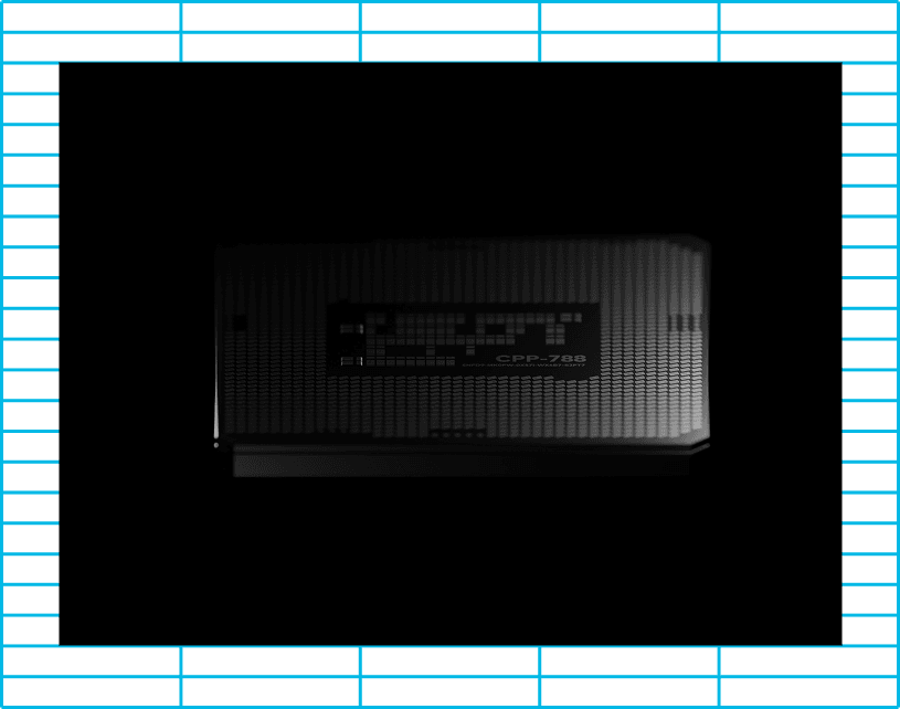
The efficient workhorse. Designed for the most tokens per USD and per kilowatt in everyday AI inference: chat, search, assistants and enterprise applications.

2027
Kuling
3 nm (planned)
Built to carry heavy loads. Designed for large reasoning models, AI agents and long context, with the lowest cost per token at scale for AI factories and sovereign AI infrastructure.

2028
Orkan
2 nm (planned)
The flagship. Designed for the largest and most demanding workloads, including frontier models, multimodal and physical AI, at maximum inference power for minimum cost and energy.
